SDG #210 Extreme LED Current Melted Solder! Using Aluminium PCBs from PCBWay
This episode continues the high power LED characterisation series, this time on purpose built aluminium backed (IMS) test boards rather than standard FR4. The question is practical: how much drive current a modern high brightness emitter can take before something in the thermal path fails, and where that failure occurs first. The answer turns out to be less about the LED die and more about the solder joint holding it down.
The build walkthrough is useful for anyone considering metal core boards for the first time. The single layer aluminium substrate is inspected closely for dielectric quality, solder mask coverage and pad finish, and the assembly is done by hand with a vacuum pick up tool and paste before reflow. Because the aluminium core spreads heat aggressively, hand soldering is impractical and the board also behaves differently on a hotplate, which is worth knowing before committing to a design. Mounting to a heatsink with thermal interface material is covered as well, since the whole benefit of an IMS board is lost if that final interface is poor.
Testing is automated with a DAQ setup logging current, forward voltage and temperature so that the curves are repeatable rather than estimated. Driving the LED far beyond its datasheet rating produces the headline result: junction and pad temperatures climb high enough to reflow the solder under the package, destroying the joint while the die itself is still conducting. For anyone designing LED lighting, the conclusion is that headroom claims mean nothing without measured thermal resistance from junction to heatsink, and that overdriving an emitter shifts the weakest link to the mechanical and electrical joint that cannot easily be inspected.
More Electronics Projects

SDG #374 Smart Home Lighting: Adding Wireless DMX to My ESP32 Controller
Adding wireless DMX to an ESP32-S3 touch dimmer using ESP-NOW, with a 16-channel receiver, pairing, smoothing and scope-verified DMX output.
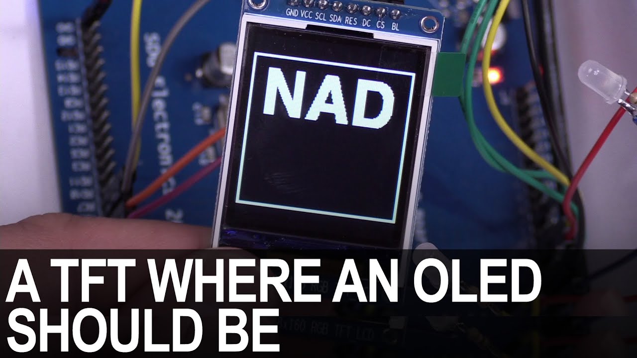
SDG #365 Reverse Engineering NAD D7050 OLED Replacement for IPS TFT
Decoding the NAD D7050's obsolete SSD1355 OLED protocol with a logic analyser, then driving an SSD1351 OLED and ST7735S IPS TFT as replacements.

SDG #360 Zero Crossing Detection and PCBWay 3D Prints
Testing PCBWay nylon PA12 and clear resin wall mounts for a Waveshare 4in ESP32-S3 touch dimmer, plus lower-power zero crossing detection options.