SDG #235 Assembling an Advent PCB Scene with PCBs from JLCPCB
This build log follows the assembly of a seasonal Advent PCB scene, a decorative Christmas display made entirely from fibreglass circuit boards that slot together into a three dimensional diorama. It is a good case study in a design style that has become popular for holiday kits: instead of a single flat board, the artwork is split across several outlines with interlocking tabs and slots, and the copper, silkscreen and exposed substrate are used as artistic layers rather than purely functional ones.
The practical interest lies in the mechanical and electrical joins. Soldering board edge to board edge is more demanding than normal through hole work, because there is little thermal mass on the pads, the joints carry structural load as well as current, and any misalignment is locked in permanently once the first fillet solidifies. Getting the slot fit right, tacking one side before committing to the second, and keeping the assembly square while working are the details that decide whether the finished scene stands straight. Board thickness tolerance matters as well, since a nominal 1.6 mm panel that arrives slightly thin or thick changes how snugly the tabs seat.
On the electronics side, the illuminated elements need current limiting and a sensible supply arrangement, and the routing has to survive being folded into three dimensions, so the trace paths across the joints deserve as much thought as the artwork.
For anyone considering a similar project, the conclusion is that decorative PCB assemblies are cheap and rewarding to prototype, but the tolerance and soldering technique on the joints, not the schematic, are where most of the effort goes. A temperature controlled iron with a decent chisel or bevel tip makes the edge joints far easier than a fine conical tip.
More Electronics Projects

SDG #374 Smart Home Lighting: Adding Wireless DMX to My ESP32 Controller
Adding wireless DMX to an ESP32-S3 touch dimmer using ESP-NOW, with a 16-channel receiver, pairing, smoothing and scope-verified DMX output.
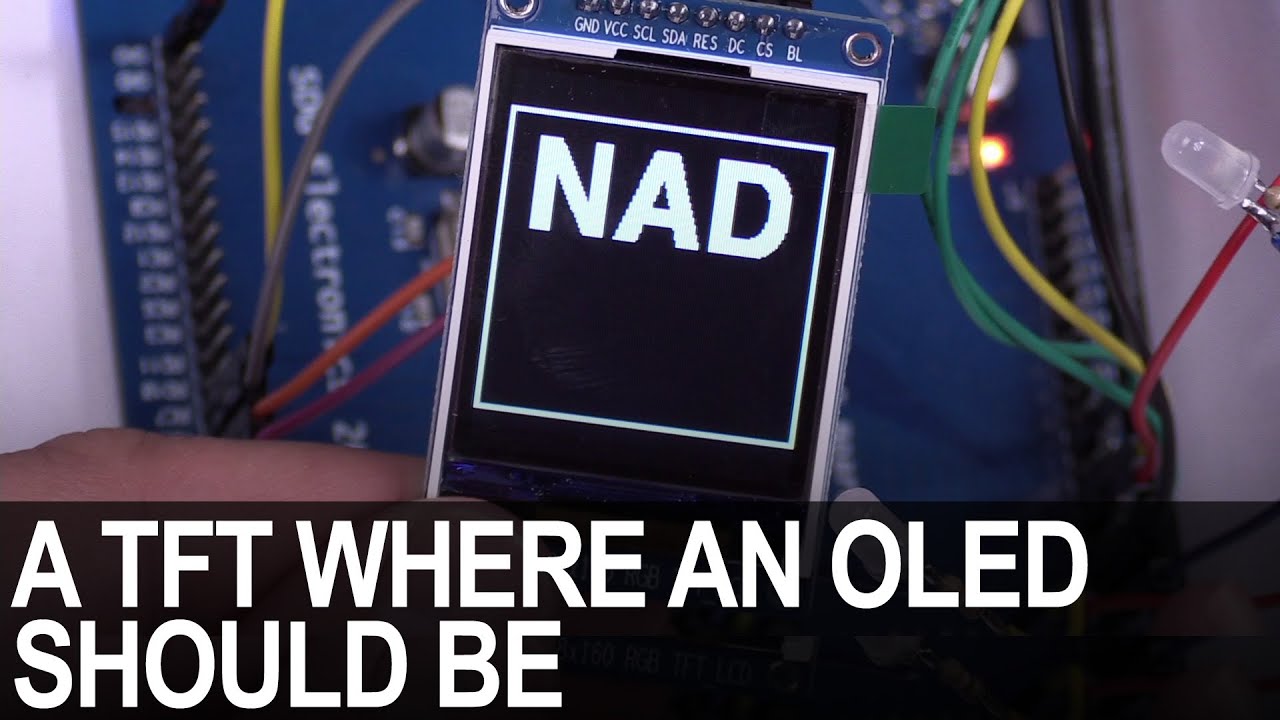
SDG #365 Reverse Engineering NAD D7050 OLED Replacement for IPS TFT
Decoding the NAD D7050's obsolete SSD1355 OLED protocol with a logic analyser, then driving an SSD1351 OLED and ST7735S IPS TFT as replacements.

SDG #360 Zero Crossing Detection and PCBWay 3D Prints
Testing PCBWay nylon PA12 and clear resin wall mounts for a Waveshare 4in ESP32-S3 touch dimmer, plus lower-power zero crossing detection options.