SDG #138 How to Panelize your PCBs
Panelising is one of the easiest ways to stretch a prototype PCB budget, and this episode works through the reasoning as well as the mechanics. When a fabricator charges per board area up to a fixed size, combining several small designs, or several copies of the same small design, into one panel means paying once and receiving many boards. The same logic applies to assembly runs, where setup and stencil costs dominate for small quantities.
The practical content covers the two mainstream depanelisation methods. V-scoring, where the fabricator cuts partway through the laminate from both faces along straight lines, gives clean edges and suits rectangular boards that share continuous cut lines. Breakaway tabs with drilled mouse bites are the alternative for irregular outlines, internal cutouts or boards that must be arranged in a non grid layout. Tab width, hole diameter and spacing all affect how easily the panel snaps and how much roughness is left on the board edge, which matters if the edge later sits in a connector slot or an enclosure groove.
Also noted are the constraints that catch people out: keeping components and copper clear of scored lines, allowing panel border rails for assembly machines, adding fiducials and tooling holes when using an SMT service, and confirming what the manufacturer will accept in terms of different designs per panel. The discussion concludes with the final cleanup after snapping, since filing or sanding mouse bite stubs is usually part of the job. For anyone ordering multiple small boards, the technique pays for itself on the first order.
More Electronics Projects

SDG #374 Smart Home Lighting: Adding Wireless DMX to My ESP32 Controller
Adding wireless DMX to an ESP32-S3 touch dimmer using ESP-NOW, with a 16-channel receiver, pairing, smoothing and scope-verified DMX output.
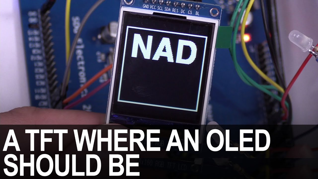
SDG #365 Reverse Engineering NAD D7050 OLED Replacement for IPS TFT
Decoding the NAD D7050's obsolete SSD1355 OLED protocol with a logic analyser, then driving an SSD1351 OLED and ST7735S IPS TFT as replacements.

SDG #360 Zero Crossing Detection and PCBWay 3D Prints
Testing PCBWay nylon PA12 and clear resin wall mounts for a Waveshare 4in ESP32-S3 touch dimmer, plus lower-power zero crossing detection options.