SDG #304 Flyback Converter Design with Power Integrations LNK562
This is the third approach to the same problem: powering a LoRa node with relays from 230V mains, needing both 5V and 3.3V rails at very low total power. The earlier capacitive dropper and non-isolated buck designs both worked, but neither offered galvanic isolation, which is a real safety consideration on a board with accessible output terminals. A flyback resolves that, and it also allows a second secondary winding so that the 3.3V rail comes directly from a centre tap rather than dissipating power in a linear regulator.
The selection process is the useful part. Working down the recommended device families, the InnoSwitch3 and TOPSwitch parts are clearly overspecified for around 2W, while the LinkSwitch and TinySwitch parts fall in the right area at roughly 50p in an 8 pin package. The LNK562 wins on simplicity: bias winding feedback instead of an optocoupler, better light load efficiency, and a clampless design that removes the primary snubber entirely.
The design spreadsheet outputs an EE16 core with 204 primary turns, a 51 turn bias winding and a centre tapped secondary, complete with layer by layer winding instructions. What it does not provide is guidance on gapping the core, which matters because a flyback stores its energy in the gap rather than transferring it continuously. That is deferred to the follow-up video.
The resulting KiCad board is deliberately oversized as a development platform, with placeholders for a primary clamp, snubbers across the output diodes and a CLC filter on the 3.3V rail, plus test points and isolation slots so that each option can be evaluated or linked out.
More Electronics Projects

SDG #374 Smart Home Lighting: Adding Wireless DMX to My ESP32 Controller
Adding wireless DMX to an ESP32-S3 touch dimmer using ESP-NOW, with a 16-channel receiver, pairing, smoothing and scope-verified DMX output.
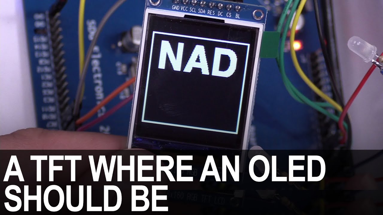
SDG #365 Reverse Engineering NAD D7050 OLED Replacement for IPS TFT
Decoding the NAD D7050's obsolete SSD1355 OLED protocol with a logic analyser, then driving an SSD1351 OLED and ST7735S IPS TFT as replacements.

SDG #360 Zero Crossing Detection and PCBWay 3D Prints
Testing PCBWay nylon PA12 and clear resin wall mounts for a Waveshare 4in ESP32-S3 touch dimmer, plus lower-power zero crossing detection options.