SDG #116 Creepage and Clearances - Adding mechanical routing to your PCB
Spacing on a mains or high voltage PCB is governed by two separate figures that are easy to confuse: clearance, the shortest path through air between two conductors, and creepage, the distance current has to travel across the surface of the board material. Creepage is usually the harder constraint because contamination, dust, humidity and carbonised tracking all make the laminate surface progressively more conductive over time. This video works through why those figures come out where they do, and what happens when the enclosure or connector layout will not allow the gap to be opened far enough.
The practical fix covered is mechanical routing: adding a milled slot or cutout in the board between the primary and secondary sides so that the surface path is interrupted entirely, forcing the leakage route around the edges of the slot. That effectively provides extra creepage distance without enlarging the board outline, which matters when a design has to fit an existing case or when isolation barriers cross under an optocoupler or transformer. There is also discussion of how routing interacts with board strength, panelisation, and what the fabricator actually needs to see in the Gerber or mechanical layer so that the slot is cut where intended rather than interpreted as a scoring line or an outline error.
The useful conclusion for anyone designing an offline supply, a solid state relay or an isolated interface board is to decide on the isolation barrier early, keep it as a clean straight line across the layout, and treat slots as a tool for tight layouts rather than a substitute for correct spacing where space allows. Standards tables, pollution degree and working voltage all feed into the figure actually required.
More Electronics Projects

SDG #374 Smart Home Lighting: Adding Wireless DMX to My ESP32 Controller
Adding wireless DMX to an ESP32-S3 touch dimmer using ESP-NOW, with a 16-channel receiver, pairing, smoothing and scope-verified DMX output.
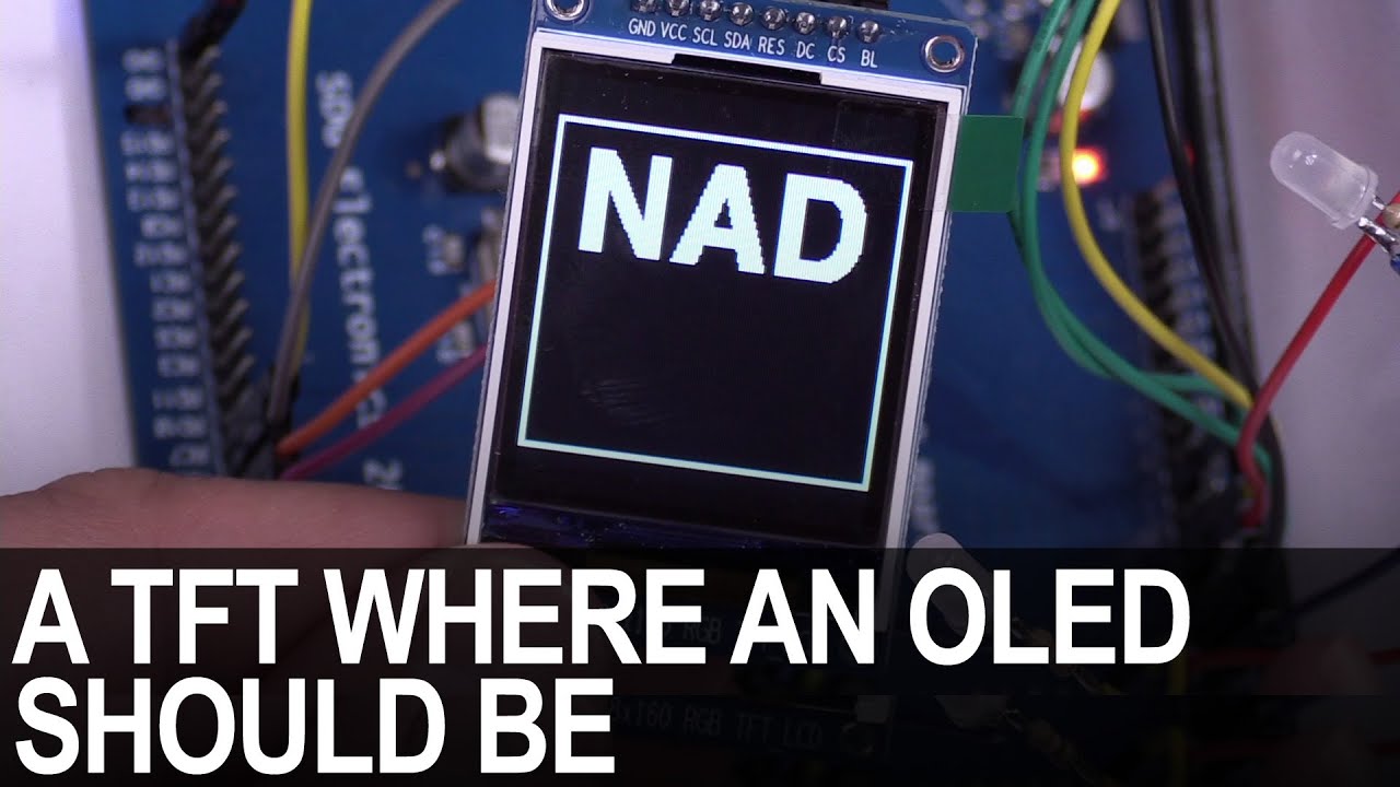
SDG #365 Reverse Engineering NAD D7050 OLED Replacement for IPS TFT
Decoding the NAD D7050's obsolete SSD1355 OLED protocol with a logic analyser, then driving an SSD1351 OLED and ST7735S IPS TFT as replacements.

SDG #360 Zero Crossing Detection and PCBWay 3D Prints
Testing PCBWay nylon PA12 and clear resin wall mounts for a Waveshare 4in ESP32-S3 touch dimmer, plus lower-power zero crossing detection options.