Calculate differential impedance, odd and even modes, coupling and near-end crosstalk.
Manufacturer stack-up referenceJLCPCB and PCBWay
Choose a board, check its layers, then apply the values you need. Two-layer presets use an estimated core thickness. Your browser remembers the selected board and signal layer.
If no value is shown, enter the dielectric constant agreed with your PCB manufacturer. These impedance models use a single value for Er.
Includes common two-layer FR-4 presets from 0.4 to 2 mm with 1 or 2 oz copper, 298 PCBWay constructions with 4 to 18 layers, and 36 JLCPCB 1.6 mm constructions with 4 or 6 layers. The JLCPCB multilayer entries use 1 oz outer copper and 0.5 oz inner copper. For other JLCPCB options, see the manufacturer’s calculator. Confirm the construction for your order. The calculations do not include solder mask or manufacturing corrections.
Result
Enter your values to calculate a result.
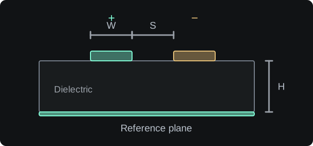
An edge-coupled differential pair
This example shows two traces above a reference plane. S is the gap between the trace edges, not the distance between their centres. The selected topology determines which dimensions are needed.
Illustration only. Not to scale.
Differential impedance
N/A
N/A
Single-ended ZoN/A
ZoddN/A
ZevenN/A
Kb (unterminated)N/A
Kb (terminated)N/A
NEXT voltage (terminated)N/A
NEXT voltage (unterminated)N/A
Saturation lengthN/A
Method and assumptions
Edge-coupled external pairs use the IPC-2141A / AN-905 coupled-microstrip expressions. Internal pairs use the Cohn coupled-stripline conformal mapping with the Wadell thickness correction. Broadside shielded pairs use electric/magnetic-wall symmetry with Cohn single-strip solutions.
Coupling coefficient: Kb = (Zeven − Zodd)/(Zeven + Zodd). NEXT is scaled by coupled length up to the saturation length Lsat = tr × vprop / 2.
Results are quasi-static and assume uniform coupled lines.
External and embedded models are most accurate for 0.1 < W/H < 3 and 0.1 < S/H < 3.
Broadside unshielded coupling is an approximation using a distant reference plane.
Find a width or gap, then check tolerances
Uses the topology, geometry and formula selected above. Change one dimension while keeping the others fixed.
Search limits are always in millimetres. The solution is applied in the calculator’s selected units. Set limits that your PCB manufacturer can produce.
Manufacturing tolerance analysis
Enter ± tolerances around the current values. These are your assumptions, not limits supplied by the selected manufacturer.
Checks every combination of low, nominal and high values for the selected parameters. This is a sensitivity estimate, not a guaranteed production limit. Height variation scales both reference-plane distances and any dielectric cover together. Gap tolerance applies only to a differential pair or coplanar line.
How spacing affects impedance and coupling
Reducing spacing increases coupling and lowers differential impedance. Changing the dielectric height affects both the single-ended impedance and the coupling. Use the target tolerance as a check, not as a guarantee.