Estimate target power-delivery impedance, plane capacitance and plane reactance.
Manufacturer stack-up referenceJLCPCB and PCBWay
Choose a board, check its layers, then apply the values you need. Two-layer presets use an estimated core thickness. Your browser remembers the selected board and signal layer.
If no value is shown, enter the dielectric constant agreed with your PCB manufacturer. These impedance models use a single value for Er.
Includes common two-layer FR-4 presets from 0.4 to 2 mm with 1 or 2 oz copper, 298 PCBWay constructions with 4 to 18 layers, and 36 JLCPCB 1.6 mm constructions with 4 or 6 layers. The JLCPCB multilayer entries use 1 oz outer copper and 0.5 oz inner copper. For other JLCPCB options, see the manufacturer’s calculator. Confirm the construction for your order. The calculations do not include solder mask or manufacturing corrections.
Result
Enter your values to calculate a result.
Power and ground planes
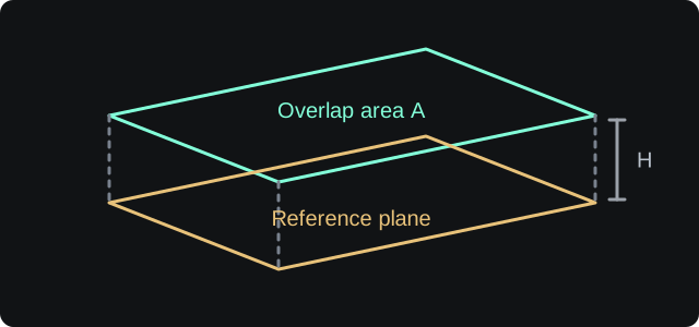
The overlapping planes form a capacitor. More area and a thinner dielectric increase the capacitance. The target impedance is calculated separately from the allowed voltage ripple and current step.
Illustration only. Not to scale.
Target PDN impedance
N/A
Plane capacitanceN/A
Capacitive reactanceN/A
Transient currentN/A
Ripple voltageN/A
Method and assumptions
Ztarget = Vripple / Itransient. Plane capacitance uses the parallel-plate relation with ε0 in pF/in: C = 0.225 × Er × A / d.
Xc = 1/(2πfC).
The plane capacitance ignores fringing, via inductance and decoupling capacitors.
This is a first-order PDN budget, not a full impedance sweep.
Comparison
Method and assumptions
Each capacitor is a series RLC branch with Z = ESR + j(ωL − 1/ωC). Component ESL and mounting inductance are added. Branch admittances are summed, together with optional ideal plane capacitance.
The plot shows a lumped approximation with constant ESR, ESL and effective capacitance. It excludes the regulator, shared connection inductance, plane resonances and distributed effects. Sampled peaks can miss very narrow resonances. Use manufacturer impedance data for detailed design.
The target impedance is the allowable ripple divided by the transient current. Plane capacitance is only one part of the power distribution network. Package, via and capacitor inductance become important at higher frequencies.