How geometry affects inductance
More turns, a larger average diameter and a larger fill factor all increase inductance. The same copper area can give different results depending on width, spacing and shape.
SDG Electronicssdgelectronics.co.uk/tools/pcb-calculator/planar-inductor/
Estimate the inductance of a planar PCB spiral from its geometry and shape.
Enter your values to calculate a result.
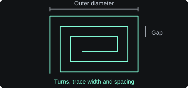
The illustration shows a square spiral. Enter the outer diameter, trace width, gap and number of turns for your chosen shape. The estimate assumes a single layer.
Illustration only. Not to scale.Inductance
N/A
Inner diameter: din = dout − 2n(w + s) + 2s. Fill factor:ρ = (dout − din)/(dout + din).
Square, hexagonal and octagonal spirals use the modified Wheeler expressionL = K1 × µ0 × n² × davg / (1 + K2 × ρ). Circular spirals use the current-sheet expression.
More turns, a larger average diameter and a larger fill factor all increase inductance. The same copper area can give different results depending on width, spacing and shape.