Follow the whole current path
A short narrow section or a small via bank can account for much of the voltage drop. Include both sides of the current loop and check thermal limits after choosing a width.
SDG Electronicssdgelectronics.co.uk/tools/pcb-calculator/power-path/
Combine outgoing and return traces with via banks to calculate voltage drop, copper losses and the width needed for your budget.
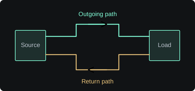
Include each copper section and via bank between the source and load, including the return path. The narrowest sections can account for much of the resistance.
Illustration only. Not to scale.Uses R = ρL/A, V = IR and P = I²R. Copper resistivity is 1.724 × 10⁻⁸ Ωm at 20 °C, with a temperature coefficient of 0.00393 per °C. Trace cross-sections are rectangular. Each via bank contains identical plated barrels in parallel.
The width estimate gives all included trace sections one common width that meets the voltage-drop budget after allowing for the vias. Check the trace current calculator separately for temperature rise. Contacts, spreading resistance and AC effects are excluded.
A short narrow section or a small via bank can account for much of the voltage drop. Include both sides of the current loop and check thermal limits after choosing a width.