SDG Electronics

Trace current and width

Estimate the current a PCB trace can carry for a chosen temperature rise, or solve for the width needed.

Inputs

Results update as you change the inputs.

Solve for
Conductor
Layer
mm

Finished copper width at the widest part of the trace.

°C
°C
mm
MHz

Use 0 for DC. Frequency only affects skin depth.

Stack-up and copper

External layers only. Internal layers are not plated.

ratio
°C
Total copper thicknessN/A

Result

Enter your values to calculate a result.

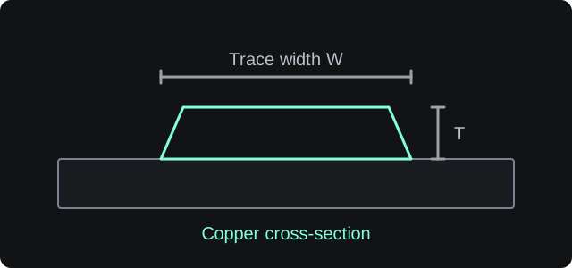
Trace cross-sectionA copper trace on a substrate, with width and thickness dimensions.WTRectangular
Input guide
Trace width and copper thickness

W is the trace width and T is the copper thickness. Together they define the copper cross-section. The allowed temperature rise sets the current estimate.

Illustration only. Not to scale.

Conductor current

N/A

Cross-sectionN/A
DC resistanceN/A
Voltage dropN/A
Power dissipationN/A
Skin depthN/A
Current densityN/A
Copper thicknessN/A
Operating temperatureN/A
Method and assumptions

Current capacity uses the IPC-2221 power-law model:I = k · ΔT0.44 · A0.725, with k = 0.048 for external layers and k = 0.024 for internal layers.A is the copper cross-section in square mils.

The result is the current that produces the selected temperature rise above ambient. It is not a fuse rating or a maximum current before failure.

  • Typical model range: ΔT 10–100 °C and cross-section up to about 700 sq mil.
  • Copper thickness is base copper plus plating on external layers only.
  • Etch factor changes the cross-section from a rectangle to a trapezoid.
  • Resistance and voltage drop use copper resistivity at the operating temperature.
  • Skin depth is shown for AC and is not used in the current calculation.

References include the IPC-2221 conductor current charts, plus the resistivity and temperature coefficient of annealed copper.

Calculate voltage drop along a complete power path

Choose an acceptable temperature rise

A PCB trace does not have a single current rating. Its capacity depends on how much temperature rise is acceptable, the copper thickness, the layer, the etch profile and the surrounding board.

Choose Current to enter a trace width and see the current that produces the selected rise. Choose Width to enter a current and solve for the width needed. External layers carry roughly twice the current of internal layers for the same geometry in this model.

What this does not model

  • Copper planes, thermal reliefs, nearby traces or airflow beyond the selected layer assumption.
  • Fusing, long-term reliability or connector and via limits.
  • High-frequency copper loss or impedance-controlled transmission-line effects.