Match the arrival times
Equal physical lengths do not always mean equal delays. Use the propagation delay for each layer and include any known package delay before deciding how much length to add.
SDG Electronicssdgelectronics.co.uk/tools/pcb-calculator/trace-delay/
Compare route delays, include package delays and calculate the length difference allowed by a skew budget.
Choose a board, check its layers, then apply the values you need. Two-layer presets use an estimated core thickness. Your browser remembers the selected board and signal layer.
If no value is shown, enter the dielectric constant agreed with your PCB manufacturer. These impedance models use a single value for Er.
| Layer | Material | Thickness (mm) | Er |
|---|
Includes common two-layer FR-4 presets from 0.4 to 2 mm with 1 or 2 oz copper, 298 PCBWay constructions with 4 to 18 layers, and 36 JLCPCB 1.6 mm constructions with 4 or 6 layers. The JLCPCB multilayer entries use 1 oz outer copper and 0.5 oz inner copper. For other JLCPCB options, see the manufacturer’s calculator. Confirm the construction for your order. The calculations do not include solder mask or manufacturing corrections.
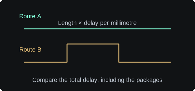
Each route can contain sections with different propagation speeds. Add their delays and any package delay before comparing arrival times.
Illustration only. Not to scale.Route delay is the sum of length multiplied by delay per millimetre for each section, plus the package delays. Skew is the absolute difference between the two routes. The suggested extra length assumes the tuning section has the entered propagation speed.
The stack-up estimate uses a microstrip or asymmetric stripline model at low frequency. It assumes the neighbouring copper layers are reference planes. Tight serpentine coupling and glass-weave effects are not modelled.
Equal physical lengths do not always mean equal delays. Use the propagation delay for each layer and include any known package delay before deciding how much length to add.