SDG #114 DC-DC Buck Regulator Converter Design, Schematic and PCB layout tutorial
This is a full length design walkthrough rather than a product review, following the build of a replacement switching power supply for an FY6900 signal generator from a blank sheet through to a finished PCB layout. The starting point is the requirement set: input voltage range, output rails, current headroom and, crucially for a signal generator, output noise. Those requirements drive the controller choice, and from there the calculations behind switching frequency, inductor value and ripple current, output capacitance and ESR, and the resistor divider that sets the feedback voltage.
The instructive part for anyone who has only ever dropped a module into a project is how many decisions sit outside the datasheet equations. Inductor saturation current versus RMS current rating, capacitor derating with DC bias, diode or synchronous rectification choices, and the thermal budget of the switch all interact. The video also covers the practical measurement side: verifying ripple and switching noise properly needs a low noise measurement setup, since probe grounding alone can produce tens of millivolts of apparent noise that is not really present.
Layout receives the attention it deserves, which is where most first attempt buck converters fail. Keeping the high di/dt loop between input capacitor, switch and diode physically small, placing the feedback tap away from the switch node, sizing copper for thermal spreading, and routing the ground return so that switching currents do not flow under sensitive traces are all demonstrated on screen.
The episode is a useful reference for moving from pre-built modules to specifying and laying out a regulator, and it explains why a cheap generic buck module often measures far worse than its ratings suggest.
More Electronics Projects

SDG #374 Smart Home Lighting: Adding Wireless DMX to My ESP32 Controller
Adding wireless DMX to an ESP32-S3 touch dimmer using ESP-NOW, with a 16-channel receiver, pairing, smoothing and scope-verified DMX output.
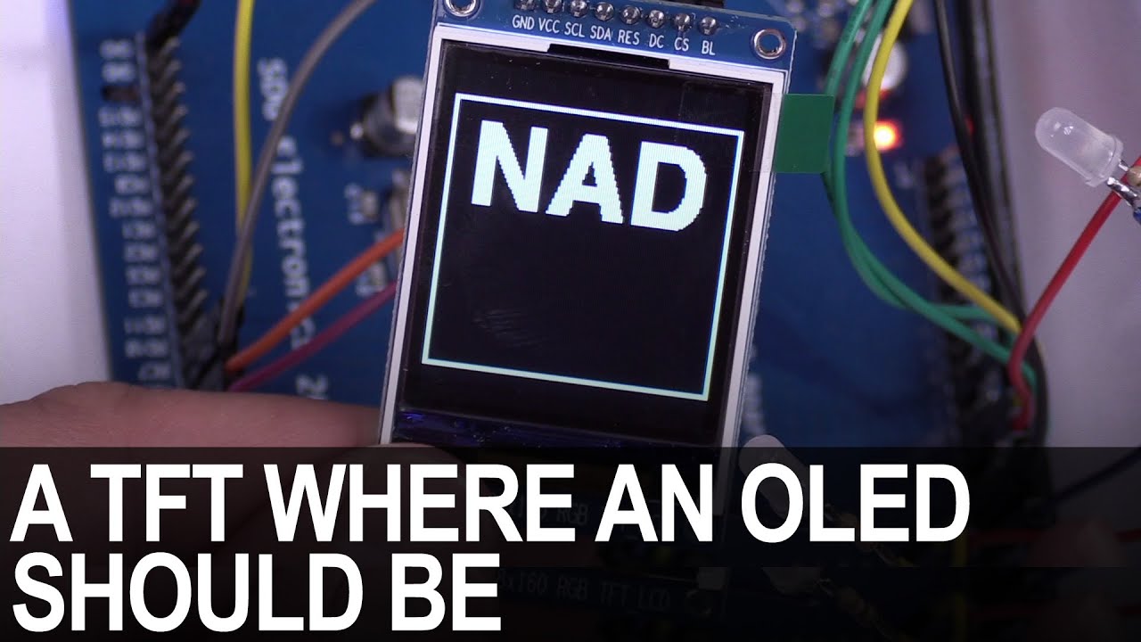
SDG #365 Reverse Engineering NAD D7050 OLED Replacement for IPS TFT
Decoding the NAD D7050's obsolete SSD1355 OLED protocol with a logic analyser, then driving an SSD1351 OLED and ST7735S IPS TFT as replacements.

SDG #360 Zero Crossing Detection and PCBWay 3D Prints
Testing PCBWay nylon PA12 and clear resin wall mounts for a Waveshare 4in ESP32-S3 touch dimmer, plus lower-power zero crossing detection options.