SDG #278 Assembling and Testing the High Current MOSFET driver
This episode moves the high current MOSFET driver project from schematic to working hardware. The newly delivered boards are inspected first, with attention to the copper pour, gate trace routing and pad geometry, all of which matter more than usual on a board expected to move large gate charges at speed. Assembly is then walked through component by component, which is useful for anyone building something similar who wants to see the practical order of operations for mixed passive and power parts.
The validation is the most instructive part. First power-up is treated cautiously, checking that the driver behaves sensibly before anything is loaded. The board then goes on a Picoscope 5000 series so that the gate waveforms can be examined properly: rise and fall times, edge quality, overshoot and ringing, and whether the driver is actually delivering the peak current the design promised. This is the sort of measurement that separates a driver that works on paper from one that will switch a large MOSFET cleanly without overheating it in the linear region.
A thermal camera pass follows, which is a quick and effective way to spot components dissipating more than expected, marginal current paths or a driver IC working harder than intended. Thermal imaging on a freshly built board frequently reveals problems that an oscilloscope trace will not.
The closing section considers where the design goes next, including the limits found during testing and the changes worth making on a revision. It is a realistic view of how much measurement is needed before a gate drive board can be trusted.
More Electronics Projects

SDG #374 Smart Home Lighting: Adding Wireless DMX to My ESP32 Controller
Adding wireless DMX to an ESP32-S3 touch dimmer using ESP-NOW, with a 16-channel receiver, pairing, smoothing and scope-verified DMX output.
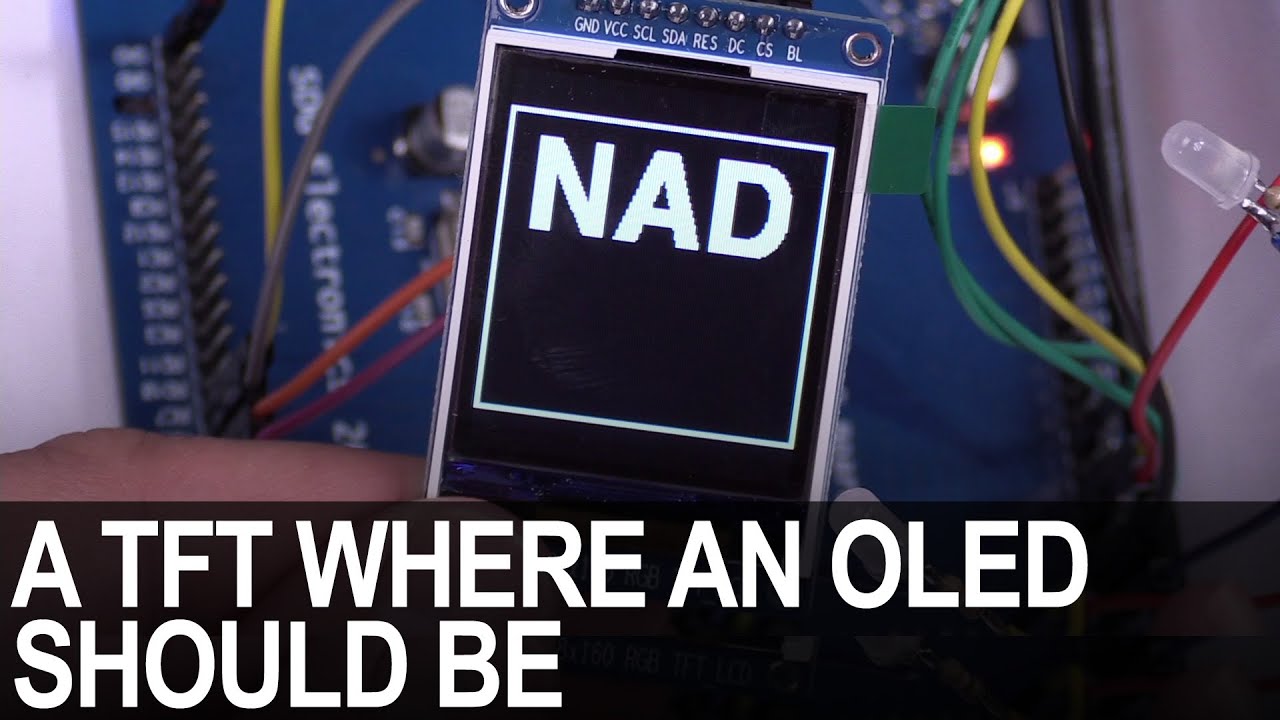
SDG #365 Reverse Engineering NAD D7050 OLED Replacement for IPS TFT
Decoding the NAD D7050's obsolete SSD1355 OLED protocol with a logic analyser, then driving an SSD1351 OLED and ST7735S IPS TFT as replacements.

SDG #360 Zero Crossing Detection and PCBWay 3D Prints
Testing PCBWay nylon PA12 and clear resin wall mounts for a Waveshare 4in ESP32-S3 touch dimmer, plus lower-power zero crossing detection options.