SDG #279 Simple Common Base MOSFET driver
This build follows on from an earlier gate driver design, replacing a dedicated driver IC with a single NPN transistor wired as a common base stage. The appeal is straightforward: the topology provides voltage gain for level shifting a 3.3V logic signal up to a full 12V gate drive, and it does so without inverting the signal, which avoids the failure mode where a glitching or resetting microcontroller unintentionally switches a heavy load on.
The trade-off is current gain below unity. Turning the MOSFET on means turning the transistor off and letting a 3k3 pull up supply only three to four milliamps of gate current; turning it off means whatever drives the emitter has to sink that current. The board is laid out with selectable zero ohm links so that both cases can be compared: driven through a buffer, and driven directly from a PIC microcontroller pin.
Oscilloscope captures show the buffered version reaching roughly 11.76V at the gate with a turn on time near five microseconds. Driving the pin directly adds a visible hump and stretches turn on toward fifteen microseconds, but the load waveform at around four amps stays clean and thermal imaging shows no measurable MOSFET heating in either configuration, which suggests that switching losses remain trivial at 200Hz.
A useful side lesson is the ringing diagnosis: an electrolytic across the supply rail removes the supply side dip caused by long leads, and a 100nF capacitor across the load absorbs the inductive turn off spike. The design needs a separate rail above the load supply, or zener clamping if the supply exceeds the MOSFET’s Vgs rating.
More Electronics Projects

SDG #374 Smart Home Lighting: Adding Wireless DMX to My ESP32 Controller
Adding wireless DMX to an ESP32-S3 touch dimmer using ESP-NOW, with a 16-channel receiver, pairing, smoothing and scope-verified DMX output.
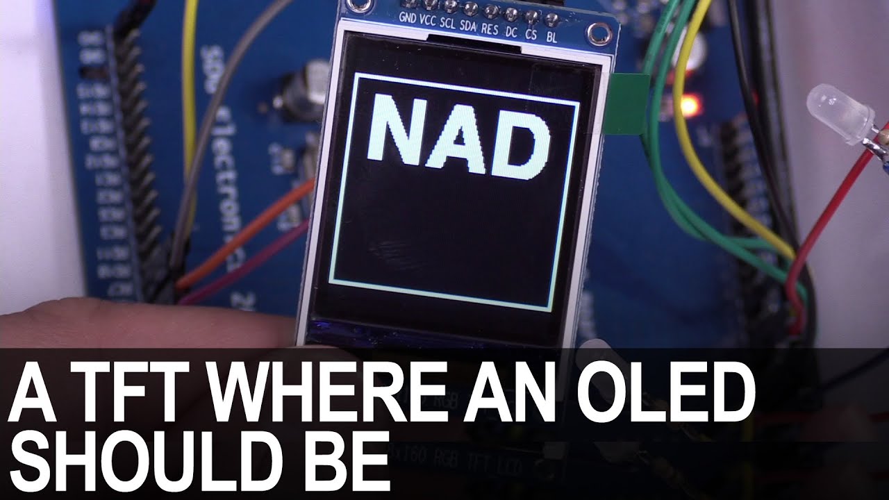
SDG #365 Reverse Engineering NAD D7050 OLED Replacement for IPS TFT
Decoding the NAD D7050's obsolete SSD1355 OLED protocol with a logic analyser, then driving an SSD1351 OLED and ST7735S IPS TFT as replacements.

SDG #360 Zero Crossing Detection and PCBWay 3D Prints
Testing PCBWay nylon PA12 and clear resin wall mounts for a Waveshare 4in ESP32-S3 touch dimmer, plus lower-power zero crossing detection options.