SDG #130 High Voltage Cockroft Walton Multiplier for ESD Simulator with PCBs from JLCPCB
This build addresses a genuinely demanding piece of analogue design: a Cockcroft-Walton voltage multiplier ladder intended to feed an ESD simulator, built on properly fabricated PCBs rather than the usual tangle of flying diodes and capacitors. The appeal of the topology is that each diode and capacitor only ever sees a fraction of the final output, so a modest AC input and a stack of cheap parts can reach the multi-kilovolt range without exotic components.
The engineering content lies in the practical constraints rather than the textbook mathematics. Board layout for kilovolt potentials means considering creepage and clearance between stages, rounding off sharp copper features that would otherwise start corona discharge, keeping the ladder physically compact enough to limit stray capacitance, and deciding where solder mask and bare substrate help or hinder. Component selection matters as well: diode reverse voltage and recovery behaviour set the usable drive frequency, while capacitor voltage rating and value determine both ripple and how much current the stack can deliver under load, which is exactly what an ESD discharge network needs.
The wider point for anyone considering a similar project is that a multiplier’s no load output looks impressive but sags quickly once real current is drawn, so the number of stages, capacitor size and drive frequency all have to be chosen together for the intended application. Anyone interested in ESD testing, high voltage experiments or simply learning how to lay out a board that will not flash over will find transferable technique here, including where a fabricated PCB genuinely beats point to point wiring and where it introduces new problems.
More Electronics Projects

SDG #374 Smart Home Lighting: Adding Wireless DMX to My ESP32 Controller
Adding wireless DMX to an ESP32-S3 touch dimmer using ESP-NOW, with a 16-channel receiver, pairing, smoothing and scope-verified DMX output.
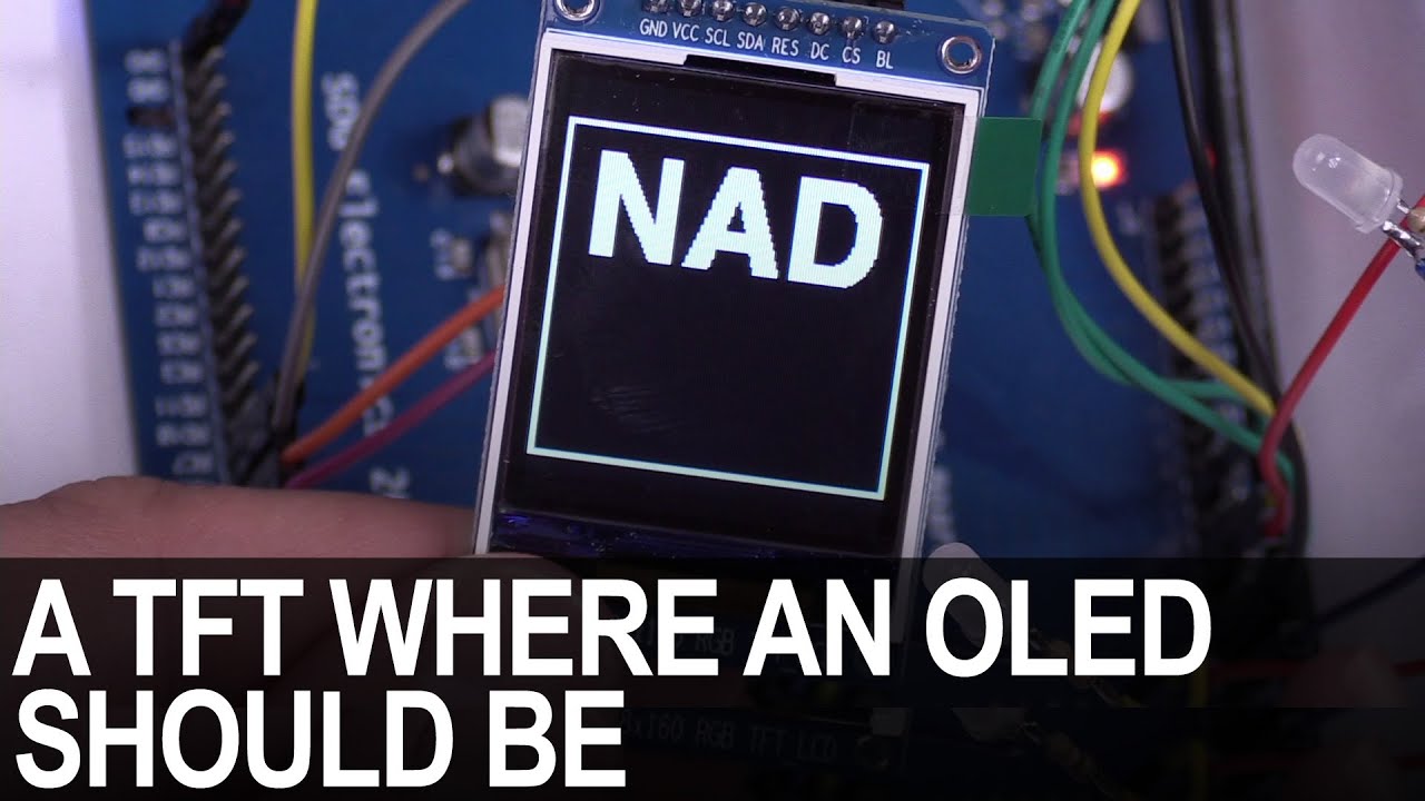
SDG #365 Reverse Engineering NAD D7050 OLED Replacement for IPS TFT
Decoding the NAD D7050's obsolete SSD1355 OLED protocol with a logic analyser, then driving an SSD1351 OLED and ST7735S IPS TFT as replacements.

SDG #360 Zero Crossing Detection and PCBWay 3D Prints
Testing PCBWay nylon PA12 and clear resin wall mounts for a Waveshare 4in ESP32-S3 touch dimmer, plus lower-power zero crossing detection options.