SDG #119 Building the DC-DC PCB for the FY6900 Signal Generator
The FY6900 is a capable, low cost arbitrary waveform generator, but its stock internal linear supply ties it to mains power and adds bulk. This build documents a custom DC-DC converter board designed to replace that arrangement, allowing the generator to run from a single DC input while still producing the split rails the analogue output stage needs.
The engineering problem is not simply generating the voltages but doing so without degrading the instrument’s output quality. Switching converters inject high frequency ripple and common mode noise, and a signal generator is exactly the sort of device where that appears immediately on an oscilloscope trace. Component selection, layout, ground return paths and output filtering all matter far more than they would on a general purpose power board, which is why the design warrants a full assembly and verification pass rather than a quick bench modification.
Assembly covers reflow and hand soldering of the SMD parts, checking for shorts before applying power, and bringing the board up carefully to confirm that each rail settles where it should under load. Measurement work then uses a differential probe to examine ripple and switching artefacts properly, since single ended probing on a floating supply readily produces misleading results.
For anyone considering a similar modification, the conclusion is that a DC-DC replacement in test equipment is realistic but needs verification with real measurements. If the generator’s noise floor and output cleanliness are unchanged, the modification is a genuine gain in portability and thermal behaviour. If not, the linear supply was doing valuable work.
More Electronics Projects

SDG #374 Smart Home Lighting: Adding Wireless DMX to My ESP32 Controller
Adding wireless DMX to an ESP32-S3 touch dimmer using ESP-NOW, with a 16-channel receiver, pairing, smoothing and scope-verified DMX output.
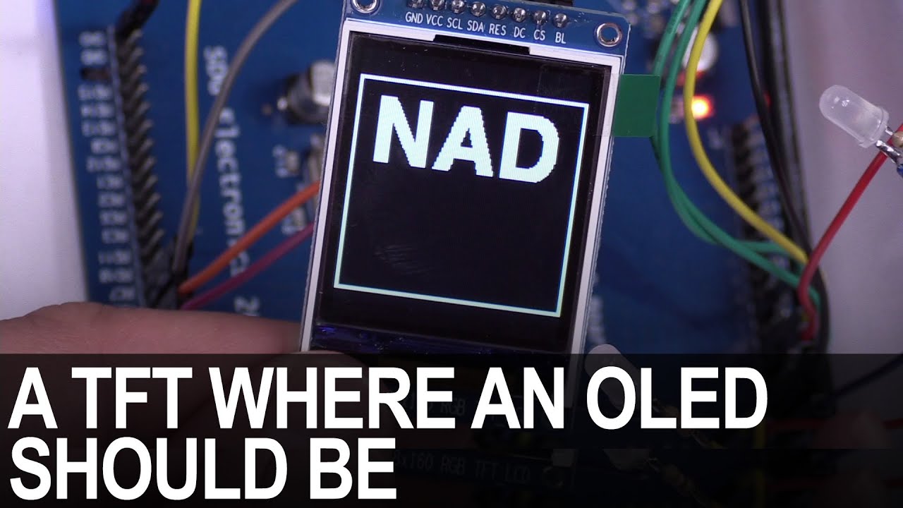
SDG #365 Reverse Engineering NAD D7050 OLED Replacement for IPS TFT
Decoding the NAD D7050's obsolete SSD1355 OLED protocol with a logic analyser, then driving an SSD1351 OLED and ST7735S IPS TFT as replacements.

SDG #360 Zero Crossing Detection and PCBWay 3D Prints
Testing PCBWay nylon PA12 and clear resin wall mounts for a Waveshare 4in ESP32-S3 touch dimmer, plus lower-power zero crossing detection options.