SDG #121 Circuit Stack LED PCBs for a 3D Effect
This build takes a simple idea, an LED populated circuit board, and adds depth by stacking several boards one behind another so that the illuminated traces and components read as a three dimensional structure rather than a flat panel. The engineering problems are not the LEDs themselves but everything around them: how to keep the layers mechanically rigid and evenly spaced, how to pass power between boards without spoiling the visual effect, and how to design the artwork on each layer so that the front boards do not simply obscure what is behind them.
Assembly is handled with reflow style techniques rather than hand soldering every part, using solder paste applied to the pads and hot air to bring the joints up to temperature. That approach deserves attention from anyone considering a similar project, because dozens of small SMD LEDs and resistors per board make manual iron work slow and inconsistent in brightness across the array. Paste volume, tip and nozzle choice, and airflow all matter here, and getting them wrong on a board with this much repetition shows immediately as tombstoned or dim parts.
The stacked approach also has practical implications for cost and turnaround, since multiple thin layers can often be ordered in a single small prototype run. For anyone building signage, badges, art pieces or display demonstrations, the conclusion is that visual impact comes mainly from spacing and layer artwork planning, not from more expensive components. It is a good weekend project that also serves as useful practice in paste and hot air assembly and board alignment.
More Electronics Projects

SDG #374 Smart Home Lighting: Adding Wireless DMX to My ESP32 Controller
Adding wireless DMX to an ESP32-S3 touch dimmer using ESP-NOW, with a 16-channel receiver, pairing, smoothing and scope-verified DMX output.
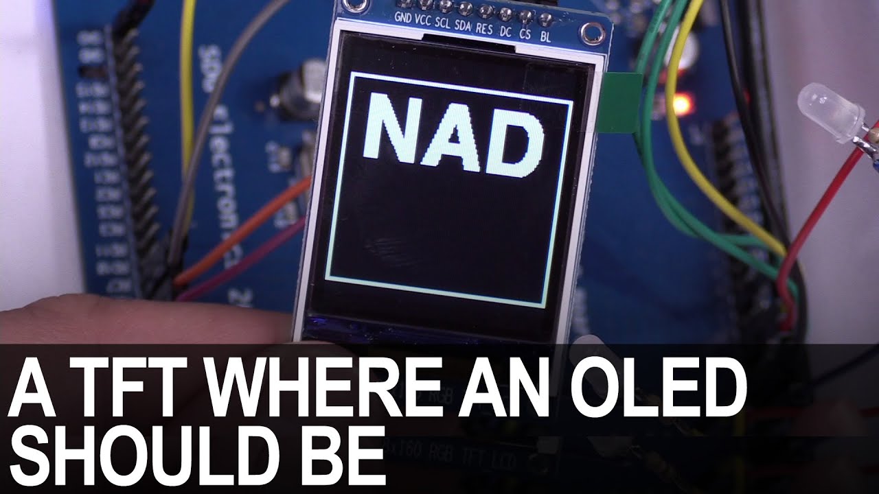
SDG #365 Reverse Engineering NAD D7050 OLED Replacement for IPS TFT
Decoding the NAD D7050's obsolete SSD1355 OLED protocol with a logic analyser, then driving an SSD1351 OLED and ST7735S IPS TFT as replacements.

SDG #360 Zero Crossing Detection and PCBWay 3D Prints
Testing PCBWay nylon PA12 and clear resin wall mounts for a Waveshare 4in ESP32-S3 touch dimmer, plus lower-power zero crossing detection options.