Choose a pad size your manufacturer can produce
Start with the finished hole and the minimum annular ring your PCB manufacturer can produce. Then check that the pad still leaves room for the conductors and spacing you need.
SDG Electronicssdgelectronics.co.uk/tools/pcb-calculator/padstack/
Calculate pad diameters, annular rings, BGA lands and conductor fit between pads.
Enter your values to calculate a result.
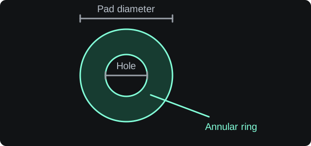
The annular ring is the copper left around the finished hole. Allow for drill and layer registration tolerances. Check the finished dimensions with your PCB manufacturer.
Illustration only. Not to scale.External layer pad
N/A
Through-hole pads use pad = hole + 2 × annular ring. Plane pads add the thermal isolation on both sides.
Conductor fit compares the chosen pad diameter with the available space between pads, allowing for the conductor width and spacing constraints.
Start with the finished hole and the minimum annular ring your PCB manufacturer can produce. Then check that the pad still leaves room for the conductors and spacing you need.