SDG Electronics

Via properties

Calculate via current, barrel resistance and the lumped electrical properties of a plated through via.

Manufacturer stack-up referenceJLCPCB and PCBWay

Choose a board, check its layers, then apply the values you need. Two-layer presets use an estimated core thickness. Your browser remembers the selected board and signal layer.

If no value is shown, enter the dielectric constant agreed with your PCB manufacturer. These impedance models use a single value for Er.

Layer details
LayerMaterialThickness (mm)Er

Includes common two-layer FR-4 presets from 0.4 to 2 mm with 1 or 2 oz copper, 298 PCBWay constructions with 4 to 18 layers, and 36 JLCPCB 1.6 mm constructions with 4 or 6 layers. The JLCPCB multilayer entries use 1 oz outer copper and 0.5 oz inner copper. For other JLCPCB options, see the manufacturer’s calculator. Confirm the construction for your order. The calculations do not include solder mask or manufacturing corrections.

Inputs

Results update as you change the inputs.

Via type

Capacitance and impedance are modelled for multilayer vias.

Geometry
mm
mm
mm
mm
mm

Used for multilayer capacitance and impedance.

Thermal & signal
°C
°C
×
:1
Material
ratio
°C

Result

Enter your values to calculate a result.

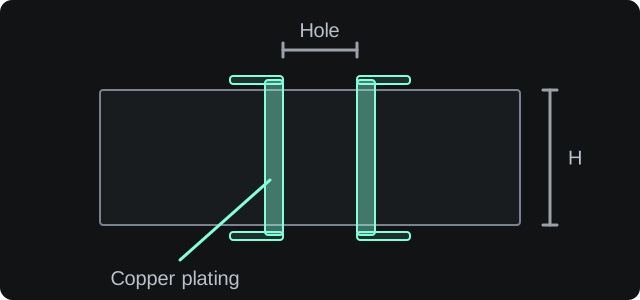
Via cross-sectionA plated via through a PCB with pads and a reference-plane opening.DHTPlated barrel + pads
Input guide
A plated via through the board

The drilled hole is lined with copper. Use the finished hole diameter, barrel plating thickness and board thickness. The pad and clearance opening affect the parasitic estimates.

Illustration only. Not to scale.

Via current

N/A

Barrel areaN/A
DC resistanceN/A
Voltage dropN/A
Power dissipationN/A
CapacitanceN/A
InductanceN/A
ImpedanceN/A
Resonant frequencyN/A
Step responseN/A
Thermal resistanceN/A
Aspect ratioN/A
Current densityN/A
Operating temperatureN/A
Outer diameterN/A
Method and assumptions

The barrel is a plated annulus. The copper cross-section isA = π/4 × ((D + 2T)² − D²).

Lumped parasitics use the Johnson/High-Speed Digital Design forms:C = 1.41 × εr × h × Dpad / (Dantipad − Dpad) pF andL = 5.08 × h × (ln(4h/d) + 1) nH, with dimensions in inches.

Impedance is √(L / (C × 0.001)), resonance is1 / (2π√(LC)), and the 10–90% step response is1.1 × C × Z.

  • Capacitance, impedance, resonance and step response are only modelled for multilayer vias.
  • Current uses the base IPC-2221 internal-layer power law. Copper planes and thermal correction factors are not included.
  • Thermal resistance is a one-dimensional copper-barrel estimate.
  • DC resistance uses copper resistivity at ambient plus temperature rise.

Via arrays for current and heat

Enter values, then compare the results.

Compare an array at your chosen load current. This calculation does not multiply a single-via current rating to predict an array rating.

mm
mm
mm
°C
A
W

Comparison

Method and assumptions

Barrel area is π(Dt + t²), where D is the finished hole diameter and t is the plating thickness. Identical barrels share current and heat equally. Resistance scales as 1/N.

Thermal conduction uses Rθ = L/(kAN), with copper conductivity k = 400 W/(m·K). The result is the temperature difference across the barrels, not junction-to-ambient temperature rise. Pads, heat spreading, solder filling, airflow and thermal interaction need separate consideration.

TI guidance on PCB copper spreading

The copper barrel sets the current capacity

A via's current capacity is set by the plated copper annulus, not the pad diameter. Increase the hole, plating thickness or allowed temperature rise to carry more current. The electrical parasitics affect high-speed signals. DC resistance and thermal resistance are important for power delivery.

What this does not model

  • Non-functional pads, plane openings, via stubs or differential via coupling.
  • Local copper planes, thermal reliefs or airflow around the via.
  • High-frequency field behaviour or a full 3D via transition.