SDG Electronics

Thermal management

Compare device junction temperatures with and without a heat sink using the thermal resistance of each arrangement.

Inputs

Results update as you change the inputs.

Ambient
°C
Device without a heat sink
°C/W
W
Device with a heat sink

Use the total thermal resistance from the junction to ambient, including the package, interface and heat sink.

°C/W
W

Result

Enter your values to calculate a result.

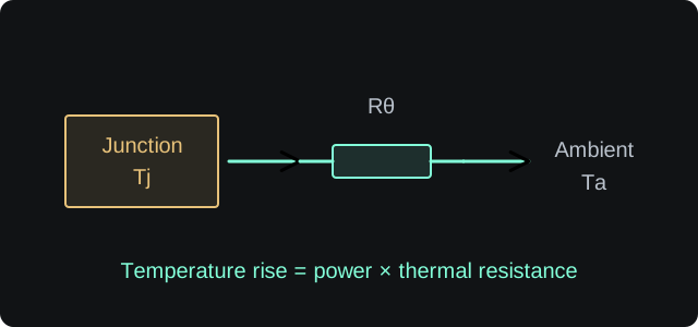
Heat flow from the junction to ambient

Power dissipation raises the junction temperature above ambient. Use a thermal resistance that represents the complete heat path for your board and mounting arrangement.

Illustration only. Not to scale.

Junction temperature without a heat sink

N/A

Without a heat sink (°C)N/A
Without a heat sink (°F)N/A
With a heat sink (°C)N/A
With a heat sink (°F)N/A
Method and assumptions

The junction temperature uses the single-resistance modelTj = Rθ × P + Tamb.

  • The thermal resistance must match the actual board, airflow and mounting condition.
  • This estimates the temperature once it has settled. Thermal capacitance and heating during a transient are not modelled.
  • Both results use the same ambient temperature. Each arrangement has its own thermal resistance and power dissipation.

Compare via arrays for current and heat

Choose a realistic thermal resistance

The arithmetic is simple. The uncertainty is almost entirely in the thermal resistance: it depends on the package, copper area, airflow, enclosure and mounting. Use the manufacturer's test condition or measured data where possible.

What this does not model

  • Transient thermal impedance or heat capacity.
  • Multiple heat paths in parallel.
  • Airflow curves, radiation or enclosure temperature rise.